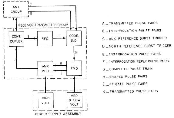
Figure 6-10.—Shipboard TACAN system, simplified block diagram.
Figure 6-11 shows how the code indicator section
would appear in a detailed block diagram for the
TACAN system shown in figure 6-10. Note that this
diagram shows the shape and amplitude of the wave
forms at various points and the location of test points.
Tube elements and pin numbers are also identified. For
example, the interrogation reply pulse (top left corner
of fig. 6-11) is applied to the grid (pin 7) of V604B, and
the output from the cathode (pin 8) of V604B is applied
to the grid (pin 2) of V611. Therefore, this kind of block
diagram is sometimes called a servicing block diagram
because it can be used to troubleshoot as well as identify
function operations. Block diagrams that break down
the simplified diagram into enough detail to show a
fairly detailed picture of functional operation, but do not
include wave forms, test points, and so on, are usually
called functional block diagrams.
Graphic electrical and electronic symbols are
frequently used in functional and detailed block
diagrams of electronic systems to present a better
picture of how the system functions. Note the graphic
symbol for the single-pole, two-position switch S603 at
the bottom left corner in figure 6-11. Figure 6-12 shows
other examples of graphic symbols in a block diagram.
Detailed block diagrams of the type shown in
figure 6-12 can be used to isolate a trouble to a
particular assembly or subassembly. However,
schematic diagrams are required to check the
individual circuits and parts.
Schematic Diagrams
Electronic schematic diagrams use graphic symbols
from ANSI Y32.2 for all parts, such as tubes, transistors,
capacitors, and inductors. Appendix III in this textbook
shows common electronic symbols from this standard.
Simplified schematic diagrams are used to show how
a particular circuit operates electronically. However,
detailed schematic diagrams are necessary for trouble-
shooting.
Figure 6-13 shows a section of the detailed
schematic diagram of the coder indicator show in fig-
ure 6-11. Some of the components in figure 6-13 are not
numbered. In an actual detailed schematic, however, all
components, such as resistors and capacitors, are
identified by a letter and a number and their values are
given. All tubes and transistors are identified by a letter
and a number and also by type. Input signals are shown
entering on the left (fig. 6-13) and signal flow is from
left to right, which is the general rule for schematic
diagrams.
In the block diagram in figure 6-11, the north
reference burst signal is shown applied to the pin 7 grid
of V601B. The pin 6 plate output of V601B is fed to the
pin 7 grid of V602, and the pin 3 cathode output of V602
6-12


